

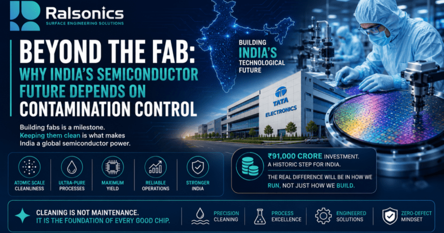
India is finally entering the semiconductor age. The Tata Electronics + ASML fab in Dholera, Gujarat will be India’s first advanced chip manufacturing facility, backed by a ₹91,000 crore investment under the India Semiconductor Mission.
It’s a historic milestone. But if we think the hard part is building the fab, we’re underestimating the challenge by an order of magnitude.
In semiconductors, the real competition starts the day after inauguration.
1. Why semiconductor manufacturing is fundamentally a cleaning problem
Unlike traditional manufacturing, where tolerances are measured in millimeters, advanced chips work at the 3-nanometer node. To put that in perspective:
Scale Comparison
3 nm Human DNA is 2.5 nm wide
20 nm The COVID virus is ∼100 nm
1 µm A speck of dust is 1000x larger than the smallest features on a chip
A speck of dust is 1000x larger than the smallest features on a chip
At this scale, manufacturing and contamination control are the same thing. A single particle landing on a wafer can bridge circuits, create shorts, and scrap the entire die.
This is why a modern semiconductor fab is also the world’s most sophisticated cleaning operation.
Key data points:
- A typical wafer undergoes 400–1000 process steps, and over 100 of those are cleaning steps
- Leading fabs run Class 1 cleanrooms, meaning less than 1 particle of 0.5 µm size per cubic foot of air
- UPW systems supply ultra-pure water at 18.2 megaohm-cm resistivity. Tap water would destroy a wafer instantly
- Chemical purity is measured in parts-per-trillion. One wrong ion can shift transistor performance
So when we say “semiconductor manufacturing,” what we really mean is “contamination-controlled manufacturing at atomic scale.”
2. The economics: Why cleanliness directly drives yield
Semiconductor economics are brutal. A single fab costs ₹75,000–₹91,000 crore to build. But the capex is just the entry ticket.
The real P&L is determined by yield, the percentage of good dies per wafer.
Here’s the math:
- A mature fab should run at 90–95% yield
- If yield drops to 85% due to contamination, a ₹91,000 Cr fab loses ₹4,500–₹9,000 Cr per year in scrapped wafers
- Downtime is worse. One hour of contamination-related shutdown in a high-volume fab can cost ₹1–2 Cr in lost output
This is why TSMC, Samsung, and Intel obsess over process control. Their moat isn’t just EUV machines. It’s the institutional knowledge of keeping 50,000 tools clean, stable, and defect-free for a decade.
In short: Yield = cleanliness. Reliability = process control. Profitability = both.
3. India’s current position and the ecosystem gap
The Government of India has recognized this. ISM 2.0 is now targeting $20 billion in semiconductor incentives, up from the initial $10 billion. This puts India closer to Korea, Japan, and Malaysia in support levels. 14 projects are already approved under ISM.
But incentives build fabs. They don’t automatically build capability.
Today, most of the critical contamination-control ecosystem sits outside India:
- Precision cleaning equipment: Megasonic, cryogenic aerosol, and plasma cleaning tools
- High-purity chemicals: 99.9999999% pure acids, solvents, and CMP slurries meeting SEMI standards
- AMC monitoring: Real-time sensors for airborne molecular contamination at ppt levels
- Talent: Process engineers who’ve debugged yield excursions for 10+ years
If India imports 100% of this ecosystem, we’ll have fabs but we’ll be dependent for yield. That’s not strategic autonomy.
4. The opportunity: Building the “second fab” around the fab
The Dholera project is the anchor. But the long-term jobs, IP, and strategic value will come from the ecosystem that keeps it running.
This includes:
- Domestic specialty chemical manufacturing for wet cleans and etch
- Precision cleaning systems engineered for Indian water, power, and humidity conditions
- Process reliability services — the “pit crews” who ensure 99.9% uptime
- Training pipelines to create Class 1 cleanroom technicians and defect engineers
India won’t become a semiconductor power by building more concrete. We’ll become a semiconductor power by building the cleanest, most reliable manufacturing environments in the world.
5. The decade ahead
The next 10 years will determine whether India is just a location for fabs, or a true semiconductor nation.
The difference will come down to process discipline. To a culture where:
- A SOP deviation stops the line, no matter what
- Data from every tool is analyzed for defect trends
- “Clean enough” is never good enough
We don’t get paid for cutting the ribbon on the fab. We get paid for every good die that ships, every single day, for 20 years.
At Ralsonics, we engineer industrial cleaning and contamination control systems for sectors where failure isn’t an option. As India builds its semiconductor base, we’re focused on building the ecosystem that keeps it running.
💬 What capability do you think India needs to build most urgently beyond the fab itself — chemicals, equipment, or talent? Share your perspective below.

