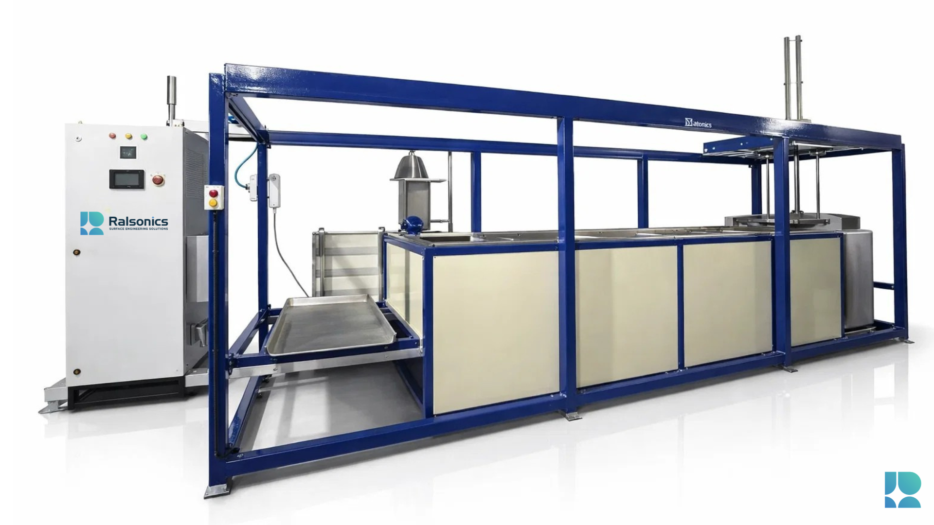
Multistage Ultrasonic Cleaner
Ralsonics delivers customized multistage ultrasonic cleaning solutions for industries that demand uncompromising quality, efficiency, and reliability.
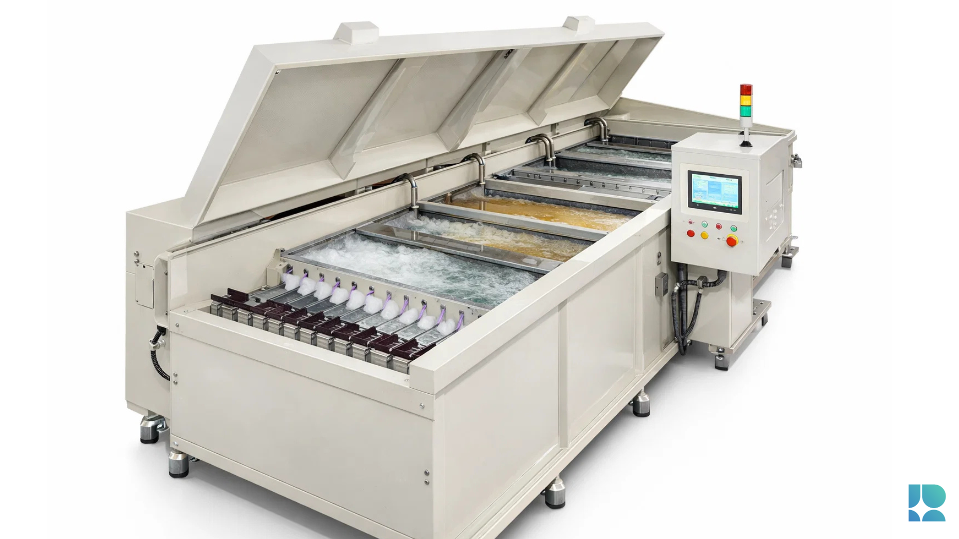
Ultrasonic Wire Cleaner
Ultrasonic Wire Cleaner effortlessly eliminates contaminants, grease, oils, and stubborn residues from wires and cables
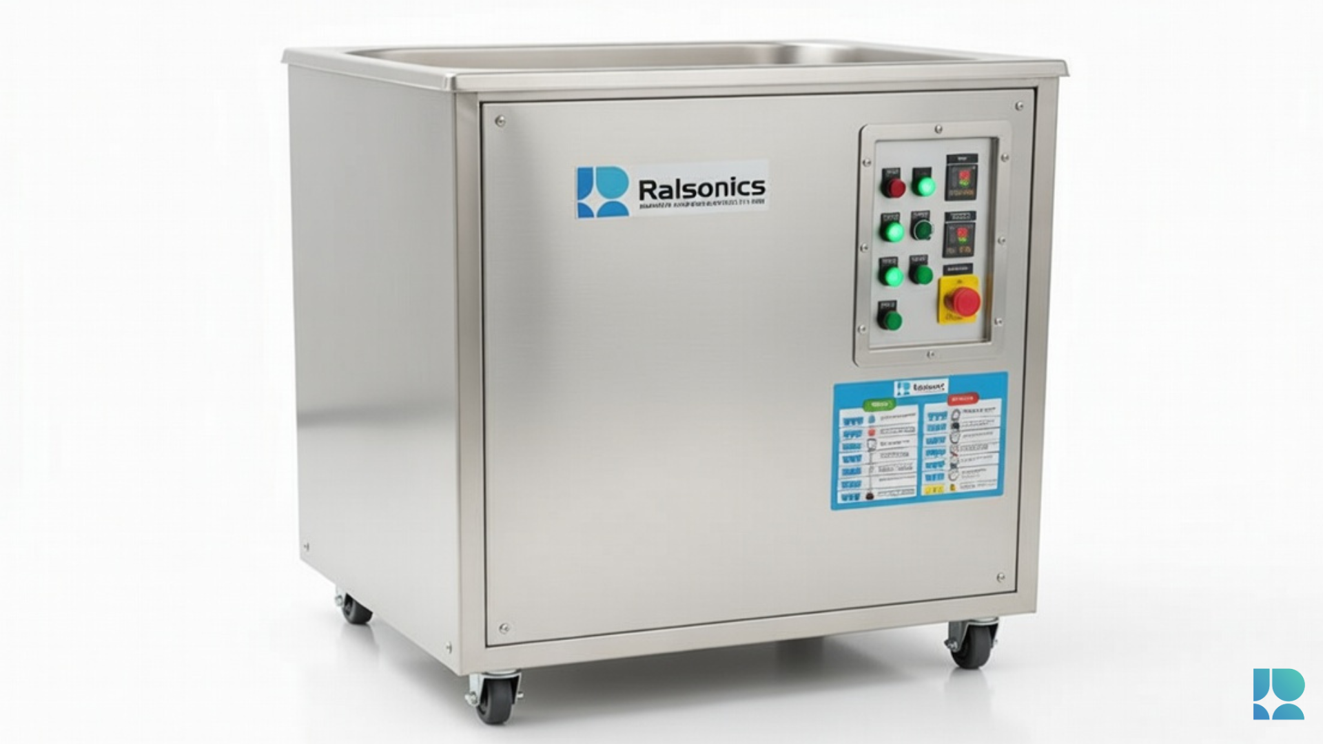
Tabletop Ultrasonic Cleaners
Ralsonics Tabletop Ultrasonic Cleaner offers a superior solution for precise and efficient cleaning on a lab scale or small scale industrial level
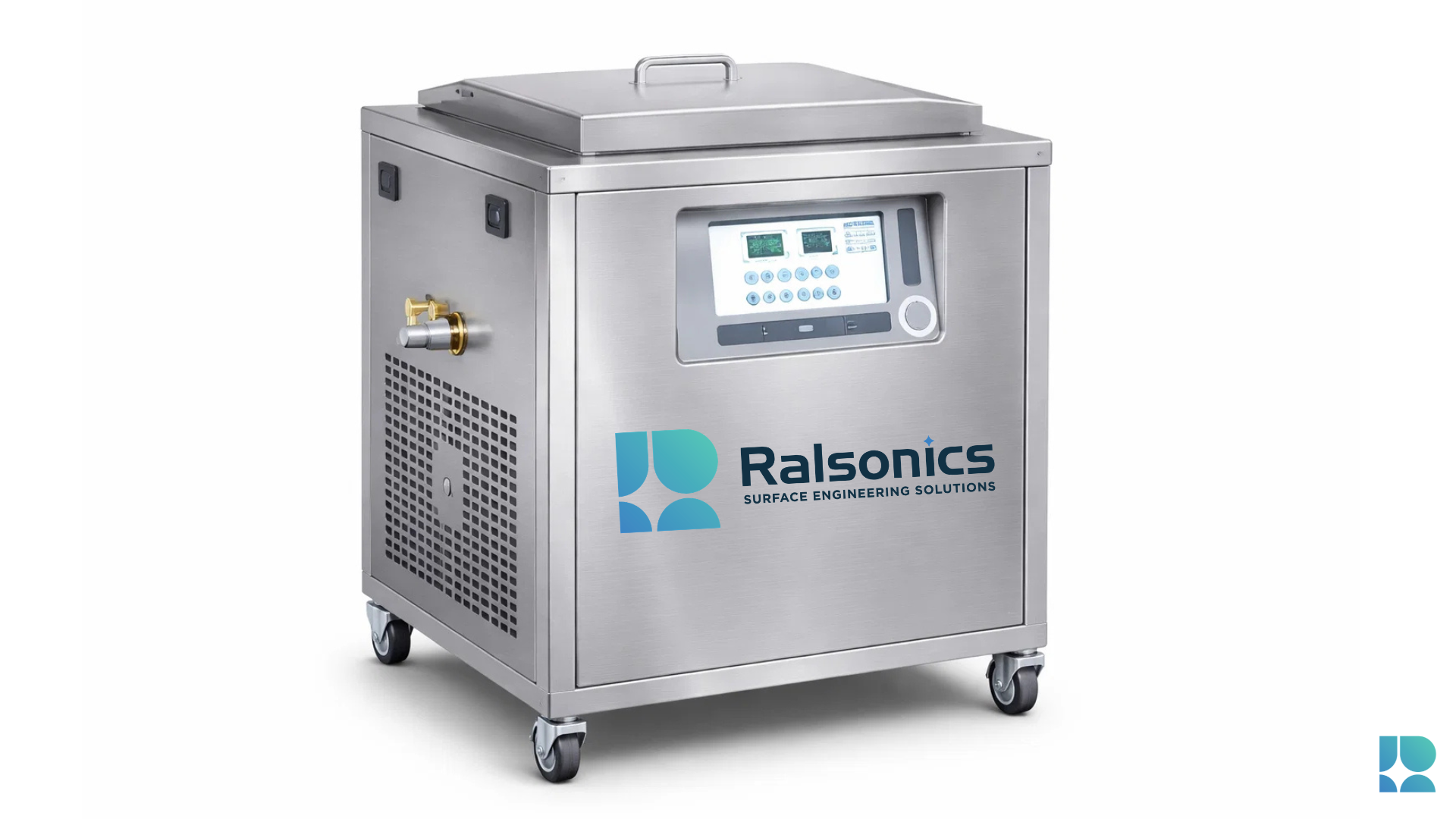
Sonicator with Chiller
A Sonicator with Chiller is a specialized ultrasonic processing system designed to deliver powerful sonication while maintaining precise temperature control.
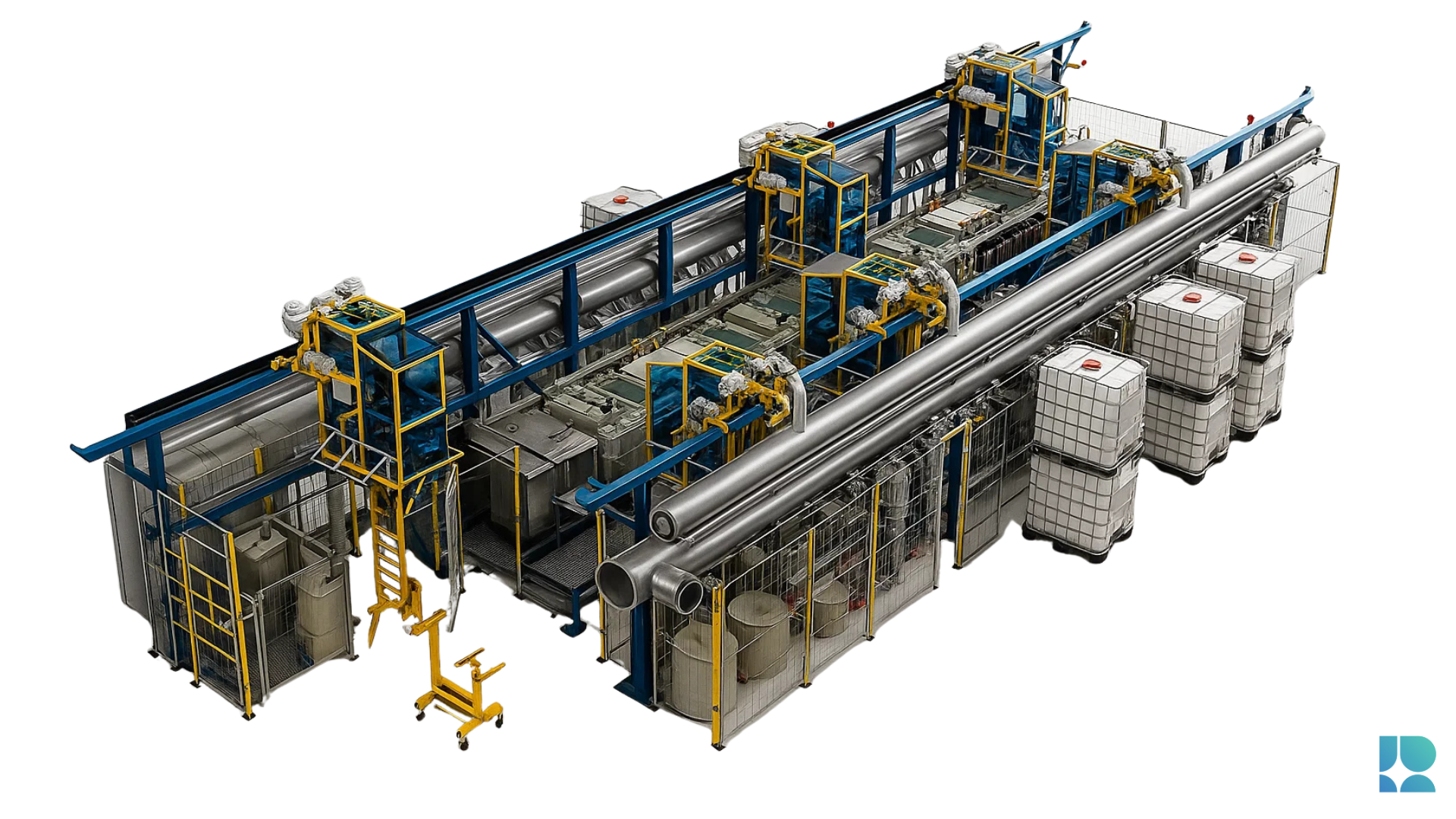
Surface Treatment Plants
A surface treatment plant combines multiple stages such as cleaning, rinsing, pickling, passivation, and drying in a controlled workflow.
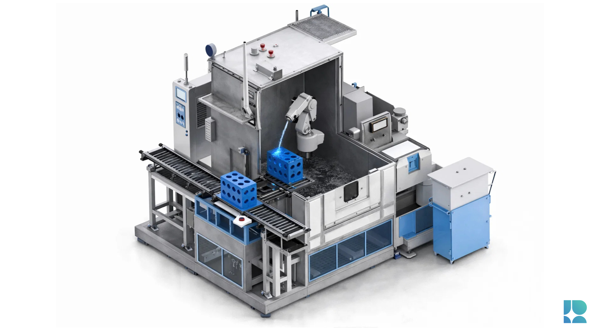
Robotic Washer
Ralsonics Robotic Washer is an advanced, fully automated industrial cleaning solution that combines robotic precision with high-pressure washing technology

Do hospitals need ultrasonic cleaners?

Role of Ultrasonic Cleaning in Aircraft Maintenance, Repair & Overhaul (MRO)

Ultrasonic Cleaning for the Pharmaceutical Industry

What is ultrasonic cleaning?